


产品详情
Positive Temperature Coefficient (PTC) Data Sheet
Description
The 2018 series provides miniature suSRace mount resettable overcurrent protection with holding current from 0.3A to 2.0A. This series is suitable for applications with applications where space is at a premium and the device current is low.
Features
|
■ RoHS compliant and lead-free ■ Halogen-free ■ Compact design saves board space |
■ Low profile ■ Fast response to fault current ■ Compatible with high temperature solders |
Applications
|
■ Mobile phones and PDAs ■ Portable MP3 and media player ■ Mobile internet Device (MID) ■ USB peripherals |
■ IC VCC protection ■ Set-top-box and HDMI ■ Game console port protection |
Electrical Characteristics
|
Part Number |
Ihold (A) |
Itrip (A) |
Vmax (Vdc) |
Imax (A) |
Pd typ. (W) |
Maximum Time To Trip |
Resistance |
||
|
Time (Sec.) |
Current (A) |
Rmin (Ω) |
R1max (Ω) |
||||||
|
SMD2018SR030 |
0.30 |
0.60 |
60 |
20 |
1.40 |
1.50 |
3.00 |
0.500 |
2.300 |
|
SMD2018SR050 |
0.55 |
1.10 |
60 |
20 |
1.40 |
2.50 |
5.00 |
0.200 |
1.000 |
|
SMD2018SR075 |
0.75 |
1.50 |
60 |
20 |
1.40 |
8.00 |
0.50 |
0.130 |
0.900 |
|
SMD2018SR100 |
1.10 |
2.20 |
15 |
40 |
1.40 |
8.00 |
0.50 |
0.100 |
0.400 |
|
SMD2018SR100/33 |
1.10 |
2.20 |
33 |
40 |
1.40 |
8.00 |
0.50 |
0.100 |
0.400 |
|
SMD2018SR150 |
1.50 |
3.00 |
15 |
40 |
1.40 |
8.00 |
1.00 |
0.070 |
0.180 |
|
SMD2018SR200 |
2.00 |
4.20 |
6 |
40 |
1.40 |
8.00 |
3.00 |
0.048 |
0.100 |
Note on Electrical Characteristics
■ Vocabulary
·Ihold = Hold current: maximum current device will pass without tripping in 23℃ still air.
·Itrip = Trip current: minimum current at which the device will trip in 23℃ still air.
·Vmax = Maximum voltage device can withstand without damage at rated current (Imax)
·Imax = Maximum fault current device can withstand without damage at rated voltage (Vmax)
·Pd typ. = Typical power dissipated from device when in the tripped state at 23℃ still air.
·Rmin = Minimum resistance of device in initial (un-soldered) state.
·R1max = Maximum resistance of device at 23℃ measured one hour after tripping or reflow soldering of 260℃ for 20 sec.
■ Value specified is determined by using the PWB with 0.090”*1.5oz copper traces.
■ Caution: Operation beyond the specified rating may result in damage and possible arcing and flame.
■ Specifications are subject to change without notice.
Polymeric PTC Selecting Guide
■ Determine the following operating parameters for the circuits:
|
·Normal operating current (Ihold) |
·Maximum interrupt current (Imax) |
|
·Maximum circuit voltage (Vmax) |
·Normal operating temperature surrounding device (min℃/max℃) |
■ Select the device from factor and dimension suitable for the application
■ Compare the maximum rating for Vmax and Imax of the PPTC device with the circuit in application and make sure
the circuit’s requirement does not exceed the device rating.
■ Check that PPTC device’s trip time (time-to-trip) will protect the circuit.
■ Verify that the circuit operating temperature is within the PPTC device’s normal operating temperature range.
■ Verify that peSRormance and suitability of the chosen PPTC device in the application.

WARNING
■ Mechanical Stress
·PPTC devices will undergo a thermal expansion during fault condition. If PPTC devices are installed or placed in an application where the space between PPTC devices and the surrounding materials (e.g., covering materials, packaging materials, encapsulate materials and the like) is insufficient, it will cause an inhibiting effect upon the thermal expansion. Pressing, twisting, bending and other kinds of mechanical stress will also adversely affect the peSRormance of the PPTC devices, and shall not be used or applied.
■ Chemical Pollutants
·Silicone-based oils, oils, solvents, gels, electrolytes, fuels, acids, and the like will adversely affect the properties of PPTC devices, and shall not be used or applied.
■ Electronic and Thermal Effect
·PPTC devices are secondary protection devices and are used solely for sporadic, accidental over-current or over-temperature error condition, and shall NOT be used if or when constant or repeated fault conditions (such fault conditions may be caused by,among others, incorrect pin-connection of a connector) or over-extensive trip events may occur.
·PPTC devices are different from fuses and, when a fault condition occurs, will go into high-resistance state and do not open circuit, in which case the voltage at such PPTC devices may reach a hazardous level.
·Operation over the maximum rating or other forms of improper use may cause failure, arcing, flame and/or other damage to the PPTC devices.
·Conductive material contamination, such as metal particle, may induce shortage, flame or arcing.
·Due to the inductance, the operation circuits may generate a circuit voltage (Ldi/dt) above the rated voltage of PPTC devices,which shall not be used under such circumstances.
■ General
·Customers shall evaluate and test the properties of PPTC devices independently to verify and ensure that their individual applications will be met.
·The peSRormance of PPTC devices will be adversely affected if they are improperly used under electronic, thermal and/or mechanical procedures and/or conditions non-conformant to those recommended by manufacturer.
·Customers shall be responsible for determining whether it is necessary to have back-up, failsafe and/or fool-proof protection To avoid or minimize damage that may result from extra-ordinary, irregular function or failure of PPTC devices.
·Any and all responsibilities and liabilities are disclaimed if any item under this notice of warning is not complied with.
Thermal Derating Curve
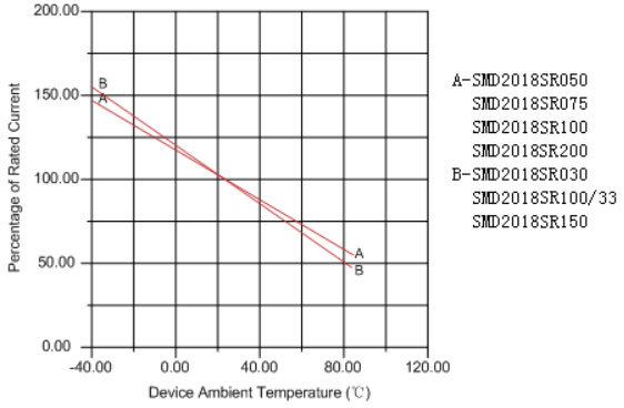
Thermal Derating Chart
Recommended Hold Current (A) at Ambient Temperature (℃)
|
Part Number |
Ambient Operation Temperature |
||||||||
|
-40℃ |
-20℃ |
0℃ |
23℃ |
40℃ |
50℃ |
60℃ |
70℃ |
85℃ |
|
|
SMD2018SR030 |
0.45 |
0.40 |
0.35 |
0.30 |
0.25 |
0.23 |
0.20 |
0.18 |
0.14 |
|
SMD2018SR050 |
0.93 |
0.80 |
0.65 |
0.50 |
0.42 |
0.38 |
0.33 |
0.30 |
0.23 |
|
SMD2018SR075 |
1.05 |
0.95 |
0.85 |
0.75 |
0.60 |
0.55 |
0.45 |
0.40 |
0.30 |
|
SMD2018SR100 |
1.66 |
1.47 |
1.29 |
1.10 |
0.91 |
0.83 |
0.73 |
0.64 |
0.50 |
|
SMD2018SR100/33 |
1.66 |
1.47 |
1.29 |
1.10 |
0.91 |
0.83 |
0.73 |
0.64 |
0.50 |
|
SMD2018SR150 |
2.26 |
2.00 |
1.76 |
1.50 |
1.24 |
1.13 |
1.00 |
0.87 |
0.68 |
|
SMD2018SR200 |
2.80 |
2.50 |
2.19 |
2.00 |
1.84 |
1.74 |
1.50 |
1.34 |
1.14 |
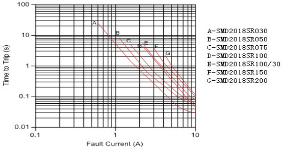
Average Time-Current Curve
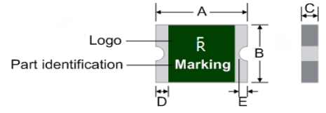
Physical Dimensions (mm)
|
Part Number |
A |
B |
C |
D |
E |
|||||
|
Min. |
Max. |
Min. |
Max. |
Min. |
Max. |
Min. |
Max. |
Min. |
Max. |
|
|
SMD2018SR030 |
4.72 |
5.44 |
3.70 |
4.43 |
0.75 |
1.25 |
0.30 |
1.50 |
0.25 |
0.65 |
|
SMD2018SR050 |
4.72 |
5.44 |
3.70 |
4.43 |
1.20 |
2.00 |
0.30 |
1.50 |
0.25 |
0.65 |
|
SMD2018SR075 |
4.72 |
5.44 |
3.70 |
4.43 |
1.20 |
2.00 |
0.30 |
1.50 |
0.25 |
0.65 |
|
SMD2018SR100 |
4.72 |
5.44 |
3.70 |
4.43 |
0.50 |
0.75 |
0.30 |
1.50 |
0.25 |
0.65 |
|
SMD2018SR100/33 |
4.72 |
5.44 |
3.70 |
4.43 |
0.75 |
1.25 |
0.30 |
1.50 |
0.25 |
0.65 |
|
SMD2018SR150 |
4.72 |
5.44 |
3.70 |
4.43 |
0.75 |
1.55 |
0.30 |
1.50 |
0.25 |
0.65 |
|
SMD2018SR200 |
4.72 |
5.44 |
3.70 |
4.43 |
0.50 |
0.75 |
0.30 |
1.50 |
0.25 |
0.65 |
Environmental Specifications
|
Operating / Storage temperature |
-40℃ to +85℃ |
|
Maximum Device SuSRace Temperature in Tripped State |
125℃ |
|
Passive Aging |
+85℃, 1000 hours ±50% typical resistance change |
|
Humidity Aging |
+85℃, 85%R.H. 1000 hours ±50% typical resistance change |
|
Thermal Shock |
MIL-STD-202, Method 107G +85℃/-40℃ 20 times -50% typical resistance change |
|
Solvent Resistance |
MIL-STD-202, Method 215 No change |
|
Vibration |
MIL-STD-883C, Method 2007.1, Condition A No change |
|
Moisture Level Sensitivity |
Level 1, J-STD-020C |
Packaging Quantity and Marking
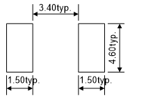
Recommended Pad Layout (mm)
|
Part Number |
Marking |
Quantity |
|
SMD2018SR030 |
030 |
1500 |
|
SMD2018SR050 |
050 |
1500 |
|
SMD2018SR075 |
075 |
1000 |
|
SMD2018SR100 |
100 |
1000 |
|
SMD2018SR100/33 |
100 |
1000 |
|
SMD2018SR150 |
150 |
1000 |
|
SMD2018SR200 |
200 |
1000 |
◎ 8mm tape on 7 inch reel per EIA-481 (equivalent to IEC286, part 3)
Physical Specifications
|
Terminal Material |
Solder-Plated Copper (Solder Material: Matte Tin (Sn)) |
|
Lead Solderability |
Meets EIA Specification RS186-9E, ANSI/J-STD-002 Category 3. |
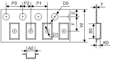
Packaging
|
Tape
|
Symbol |
Dimensions (mm) |
||
|
|
|
|
||
|
W |
12.0±0.30 |
12.0±0.30 |
12.0±0.30 |
|
|
F |
5.50±0.05 |
5.50±0.05 |
5.50±0.05 |
|
|
E1 |
1.75±0.10 |
1.75±0.10 |
1.75±0.10 |
|
|
D0 |
1.55±0.05 |
1.55±0.05 |
1.55±0.05 |
|
|
D1 |
1.50(MIN) |
1.50±0.10 |
1.50±0.10 |
|
|
P0 |
4.00±0.10 |
4.00±0.10 |
4.00±0.10 |
|
|
P1 |
8.00±0.10 |
8.00±0.10 |
8.00±0.10 |
|
|
P2 |
2.00±0.05 |
2.00±0.05 |
2.00±0.05 |
|
|
A0 |
4.40±0.10 |
4.48±0.10 |
4.45±0.10 |
|
|
B0 |
5.50±0.10 |
5.40±0.10 |
5.48±0.10 |
|
|
T |
0.25±0.10 |
0.25±0.10 |
0.25±0.10 |
|
|
K0 |
0.75±0.10 |
1.28±0.10 |
1.86±0.10 |
|
|
Leader min. |
390 |
390 |
390 |
|
|
Trailer min. |
160 |
160 |
160 |
|
|
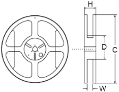
Reel
|
C |
Φ178.0±1.0 |
||
|
D |
Φ60.2±0.5 |
|||
|
H |
16.0±0.5 |
|||
|
W |
13.2±1.5 |
|||
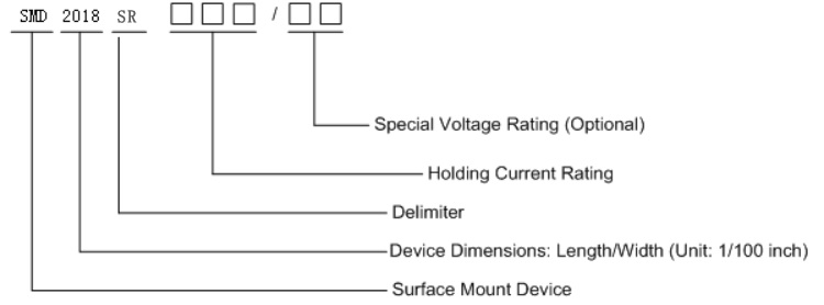
Part Number System
关键词: